 | –≠–ª–µ–∫—Ç—Ä–æ–Ω–Ω—ã–π –∫–æ–º–ø–æ–Ω–µ–Ω—Ç: LTC3406 | –°–∫–∞—á–∞—Ç—å:  PDF PDF  ZIP ZIP |
1
LTC3418
3418f
8A, 4MHz, Monolithic
Synchronous Step-Down
Regulator
High Efficiency: Up to 95%
8A Output Current
2.25V to 5.5V Input Voltage Range
Low R
DS(ON)
Internal Switch: 35m
Tracking Input to Provide Easy Supply Sequencing
Programmable Frequency: 300kHz to 4MHz
0.8V ±1% Reference Allows Low Output Voltage
Quiescent Current: 380µA
Selectable Forced Continuous/Burst Mode
Æ
Operation
with Adjustable Burst Clamp
Synchronizable Switching Frequency
Low Dropout Operation: 100% Duty Cycle
Power Good Output Voltage Monitor
Overtemperature Protected
38-Lead Low Profile (0.75mm) Thermally Enhanced
QFN (5mm ◊ 7mm) Package
Microprocessor, DSP and Memory Supplies
Distributed 2.5V, 3.3V and 5V Power Systems
Automotive Applications
Point of Load Regulation
Notebook Computers
DESCRIPTIO
U
FEATURES
APPLICATIO S
U
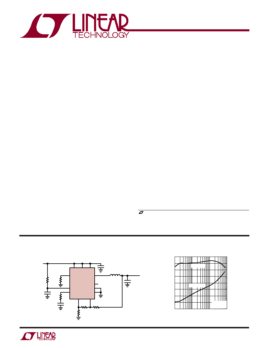
TYPICAL APPLICATIO
U
2.5V/8A Step-Down Regulator
The LTC
Æ
3418 is a high efficiency, monolithic synchro-
nous step-down DC/DC converter utilizing a constant
frequency, current mode architecture. It operates from an
input voltage range of 2.25V to 5.5V and provides a
regulated output voltage from 0.8V to 5V while delivering
up to 8A of output current. The internal synchronous
power switch increases efficiency and eliminates the need
for an external Schottky diode. Switching frequency is set
by an external resistor or can be synchronized to an
external clock. OPTI-LOOP
Æ
compensation allows the
transient response to be optimized over a wide range of
loads and output capacitors.
The LTC3418 can be configured for either Burst Mode
operation or forced continuous operation. Forced continu-
ous operation reduces noise and RF interference while
Burst Mode operation provides high efficiency by reduc-
ing gate charge losses at light loads. In Burst Mode
operation, external control of the burst clamp level allows
the output voltage ripple to be adjusted according to the
requirements of the application. A tracking input in the
LTC3418 allows for proper sequencing with respect to
another power supply.
, LTC and LT are registered trademarks of Linear Technology Corporation.
Burst Mode and OPTI-LOOP are registered trademarks of Linear Technology Corporation.
All other trademarks are the property of their respective owners.
Protected by U.S. Patents, including 5481178, 6580258, 6304066, 6127815, 6498466, 6611131,
6724174.
Efficiency and Power Loss vs Load Current
SV
IN
TRACK
R
T
C
IN
100µF
0.2µH
LTC3418
RUN/SS
I
TH
PGOOD
SW
PGND
SGND
SYNC/MODE V
FB
332
PV
IN
820pF
3418 TA01a
1000pF
C
OUT
100µF
◊2
V
OUT
2.5V
8A
4.32k
1.69k
30.1k
2.2M
V
IN
2.8V TO 5.5V
4.99k
LOAD CURRENT (A)
0.01
60
EFFICIENCY (%)
POWER LOSS (mW)
80
100
0.1
1
10
3418 TA01b
40
50
70
90
30
20
1000
100000
100
10000
10
1
EFFICIENCY
POWER LOSS
V
IN
= 3.3V
V
OUT
= 2.5V
2
LTC3418
3418f
ORDER PART NUMBER
(Note 1)
Input Supply Voltage .................................. ≠ 0.3V to 6V
I
TH
, RUN/SS, V
FB
Voltages ......................... ≠ 0.3V to V
IN
SYNC/MODE Voltages ............................... ≠ 0.3V to V
IN
TRACK Voltage .......................................... ≠0.3V to V
IN
SW Voltage .................................. ≠ 0.3V to (V
IN
+ 0.3V)
Operating Ambient Temperature Range
(Note 2) .............................................. ≠ 40∞C to 85∞C
Junction Temperature (Note 5) ............................. 125∞C
Storage Temperature Range ................. ≠65∞C to 125∞C
LTC3418EUHF
T
JMAX
= 125∞C,
JA
= 34∞C/W,
JC
= 1∞C/W
EXPOSED PAD (PIN 39) IS PGND AND MUST BE SOLDERED TO PCB
ABSOLUTE
M
AXI
M
U
M
RATINGS
W
W
W
U
PACKAGE/ORDER I
N
FOR
M
ATIO
N
W
U
U
SYMBOL
PARAMETER
CONDITIONS
MIN
TYP
MAX
UNITS
V
IN
Input Voltage Range
2.25
5.5
V
V
FB
Regulated Feedback Voltage
0∞C T
A
85∞C
0.792
0.800
0.808
V
(Note 3)
0.784
0.800
0.816
V
I
FB
Feedback Input Current
100
200
nA
V
FB
Reference Voltage Line Regulation
V
IN
= 2.5V to 5.5V (Note 3)
0.04
0.2
%/V
V
LOADREG
Output Voltage Load Regulation
Measured in Servo Loop, V
ITH
= 0.36V
0.02
0.2
%
Measured in Servo Loop, V
ITH
= 0.84V
≠0.02
≠0.2
%
V
TRACK
Tracking Voltage Offset
V
TRACK
= 0.4V
15
mV
Tracking Voltage Range
0
0.8
V
I
TRACK
TRACK Input Current
100
200
nA
V
PGOOD
Power Good Range
±7.5
±9
%
R
PGOOD
Power Good Resistance
100
150
I
Q
Input DC Bias Current
(Note 4)
Active Current
V
FB
= 0.7V, V
ITH
= 1V
380
450
µA
Shutdown
V
RUN
= 0V
0.03
1.5
µA
The
indicates specifications which apply over the full operating
temperature range, otherwise specifications are at T
A
= 25∞C. V
IN
= 3.3V. (Note 2)
Consult LTC Marketing for parts specified with wider operating temperature ranges.
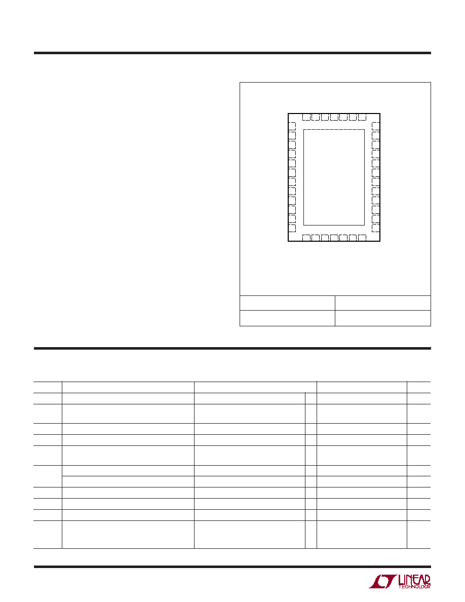
13 14 15 16
TOP VIEW
39
UHF PACKAGE
38-LEAD (7mm ◊ 5mm) PLASTIC QFN
17 18 19
38 37 36 35 34 33 32
24
25
26
27
28
29
30
31
8
7
6
5
4
3
2
1
SW
SW
PV
IN
PV
IN
PGOOD
R
T
RUN/SS
SGND
PV
IN
PV
IN
SW
SW
SW
SW
PV
IN
PV
IN
SYNC/MODE
I
TH
V
FB
SV
IN
PV
IN
PV
IN
SW
SW
PGND
PGND
PGND
TRACK
PGND
PGND
PGND
PGND
PGND
PGND
V
REF
PGND
PGND
PGND
23
22
21
20
9
10
11
12
ELECTRICAL CHARACTERISTICS
UH PART MARKING
3418
3
LTC3418
3418f
SYMBOL
PARAMETER
CONDITIONS
MIN
TYP
MAX
UNITS
f
OSC
Switching Frequency
R
OSC
= 69.8k
0.88
1
1.12
MHz
Switching Frequency Range
(Note 6)
0.3
4
MHz
f
SYNC
SYNC Capture Range
(Note 6)
0.3
4
MHz
R
PFET
R
DS(ON)
of P-Channel FET
I
SW
= 600mA
35
50
m
R
NFET
R
DS(ON)
of N-Channel FET
I
SW
= ≠ 600mA
25
35
m
I
LIMIT
Peak Current Limit
12
17
A
V
UVLO
Undervoltage Lockout Threshold
1.75
2
2.25
V
V
REF
Reference Output
1.219
1.250
1.281
V
I
LSW
SW Leakage Current
V
RUN
= 0V, V
IN
= 5.5V
0.1
1
µA
V
RUN
RUN Threshold
0.5
0.65
0.8
V
The
indicates specifications which apply over the full operating
temperature range, otherwise specifications are at T
A
= 25∞C. V
IN
= 3.3V. (Note 2)
ELECTRICAL CHARACTERISTICS
Note 1: Absolute Maximum Ratings are those values beyond which the life
of a device may be impaired.
Note 2: The LTC3418 is guaranteed to meet performance specifications
from 0
o
C to 70
o
C. Specifications over the ≠40∞C to 85∞C operating
temperature range are assured by design, characterization and correlation
with statistical process controls.
Note 3: The LTC3418 is tested in a feedback loop that adjusts V
FB
to
achieve a specified error amplifier output voltage (I
TH
).
Note 4: Dynamic supply current is higher due to the internal gate charge
being delivered at the switching frequency.
Note 5: T
J
is calculated from the ambient temperature T
A
and power
dissipation P
D
as follows:
LTC3418: T
J
= T
A
+ (P
D
)(34∞C/W)
Note 6: This parameter is guaranteed by design and characterization.
TYPICAL PERFOR A CE CHARACTERISTICS
U
W
Switch On-Resistance
vs Input Voltage
INPUT VOLTAGE (V)
2.25
0
ON-RESISTANCE (m
)
5
15
20
25
4.25
45
3418 G01
10
3.25
2.75
4.75
3.75
5.25
30
PFET
NFET
35
40
On-Resistance vs Temperature
TEMPERATURE (∞C)
≠40
0
ON-RESISTANCE (m
)
5
15
20
25
50
35
0
40
60
3418 G02
10
40
45
30
PFET
NFET
≠20
20
80
100 120
V
IN
= 3.3V
TEMPERATURE (∞C)
≠40 ≠20
REFERENCE VOLTAGE (V)
0.7980
0.7990
120
3418 G07
0.7970
0.7960
0
20
40
60
100
80
0.8000
0.7975
0.7985
0.7965
0.7995
V
IN
= 3.3V
Internal Reference Voltage
vs Temperature
T
A
= 25∞C unless otherwise noted.
4
LTC3418
3418f
TYPICAL PERFOR A CE CHARACTERISTICS
U
W
Quiescent Current
vs Input Voltage
INPUT VOLTAGE (V)
2.5
0
QUIESCENT CURRENT (
µ
A)
100
200
300
3
3.5
4
4.5
3418 G04
5
400
500
50
150
250
350
450
5.5
INPUT VOLTAGE (V)
2.25
0
LEAKAGE CURRENT (nA)
0.5
1.5
2.0
2.5
4.25
5.0
4.5
3418 G03
1.0
3.25
2.75
4.75
3.75
5.25
3.0
PFET
NFET
3.5
4.0
Switch Leakage vs Input Voltage
Frequency vs Input Voltage
INPUT VOLTAGE (V)
2.25
900
FREQUENCY (kHz)
920
960
980
1000
4.25
1100
1080
3418 G05
940
3.25
2.75
4.75
3.75
5.25
1020
1040
1060
TEMPERATURE (∞C)
≠40
900
FREQUENCY (kHz)
920
960
980
1000
1100
1040
0
40
60
3418 G06
940
1060
1080
1020
≠20
20
80
100 120
V
IN
= 3.3V
Frequency vs Temperature
Frequency vs R
OSC
R
OSC
(k)
10
0
FREQUENCY (kHz)
500
1500
2000
2500
170
4500
3418 G08
1000
90
50
210
130
250
3000
3500
4000
V
IN
= 3.3V
Efficiency and Power Loss
vs Load Current
Efficiency vs Load Current
LOAD CURRENT (A)
0.01
40
EFFICIENCY (%)
50
60
70
80
0.1
1
10
3418 G10
30
20
10
0
90
100
Burst Mode OPERATION
FORCED CONTINUOUS
V
IN
= 3.3V
V
OUT
= 2.5V
Efficiency vs Load Current
LOAD CURRENT (A)
0.01
40
EFFICIENCY (%)
50
60
70
80
0.1
1
10
3418 G11
30
20
10
0
90
100
3.3V
5V
FORCED CONTINUOUS
V
OUT
= 2.5V
Efficiency vs Load Current
LOAD CURRENT (A)
0.01
40
EFFICIENCY (%)
50
60
70
80
0.1
1
10
3418 G12
30
20
10
0
90
100
3.3V
5V
Burst Mode OPERATION
V
OUT
= 2.5V
LOAD CURRENT (A)
0.01
60
EFFICIENCY (%)
POWER LOSS (mW)
80
100
0.1
1
10
3418 TA01b
40
50
70
90
30
20
1000
100000
100
10000
10
1
EFFICIENCY
POWER LOSS
V
IN
= 3.3V
V
OUT
= 2.5V
T
A
= 25∞C unless otherwise noted.
5
LTC3418
3418f
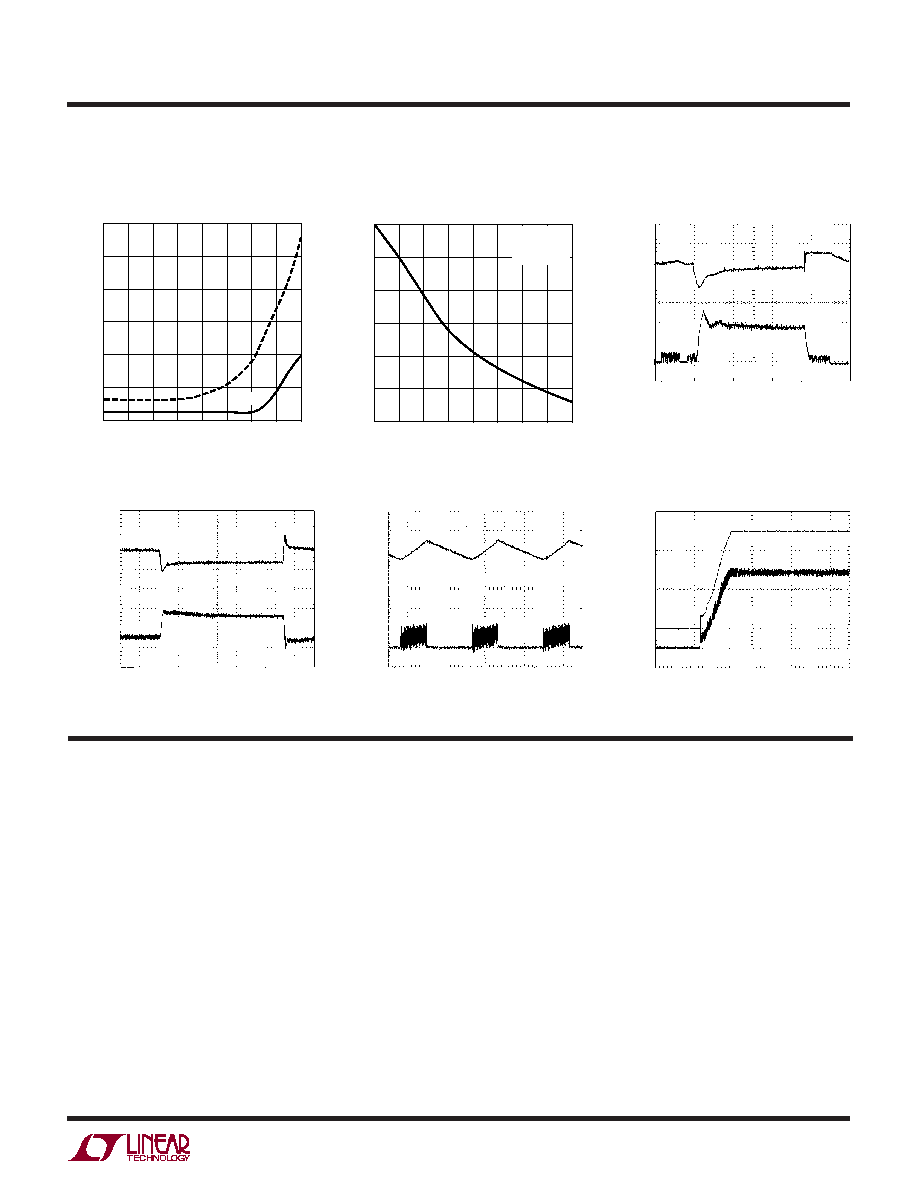
Load Regulation
Peak Inductor Current
vs Burst Clamp Voltage
V
BCLAMP
(V)
0
0
PEAK INDUCTOR CURRENT (A)
2
4
6
8
0.2
0.4
0.6
0.8
3418 G13
10
12
0.1
0.3
0.5
0.7
3.3V
5V
LOAD CURRENT (A)
0
≠0.30
V
OUT
/V
OUT
(%)
≠0.25
≠0.20
≠0.15
≠0.10
2
4
6
8
3418 G14
≠0.05
0
1
3
5
7
V
IN
= 3.3V
V
OUT
= 1.8V
f = 1MHz
Load Step Transient
OUTPUT
VOLTAGE
100mV/DIV
INDUCTOR
CURRENT
5A/DIV
20µs/DIV
V
IN
= 3.3V
V
OUT
= 2.5V
LOAD STEP: 800mA TO 8A
3418 G15
Load Step Transient
OUTPUT
VOLTAGE
100mV/DIV
INDUCTOR
CURRENT
5A/DIV
40µs/DIV
V
IN
= 3.3V
V
OUT
= 2.5V
LOAD STEP: 3A TO 8A
3418 G16
Burst Mode Operation
Start-Up Transient
OUTPUT
VOLTAGE
100mV/DIV
INDUCTOR
CURRENT
1A/DIV
20µs/DIV
V
IN
= 3.3V
V
OUT
= 2.5V
LOAD: 200mA
3418 G17
OUTPUT
VOLTAGE
500mV/DIV
INDUCTOR
CURRENT
2A/DIV
1ms/DIV
V
IN
= 3.3V
V
OUT
= 2.5V
LOAD: 8A
3418 G18
SW (Pins 1, 2, 11, 12, 20, 21, 30, 31): Switch Node
Connection to Inductor. This pin connects to the drains of
the internal main and synchronous power MOSFET
switches.
PV
IN
(Pins 3, 4, 9, 10, 22, 23, 28, 29): Power Input
Supply. Decouple this pin to PGND with a capacitor.
PGOOD (Pin 5): Power Good Output. Open-drain logic
output that is pulled to ground when the output voltage is
not within ±7.5% of regulation point.
R
T
(Pin 6): Oscillator Resistor Input. Connecting a resistor
to ground from this pin sets the switching frequency.
RUN/SS (Pin 7): Run Control and Soft-Start Input. Forcing
this pin below 0.5V shuts down the LTC3418. In shutdown
all functions are disabled drawing <1.5µA of supply cur-
rent. A capacitor to ground from this pin sets the ramp
time to full output current.
SGND (Pin 8): Signal Ground. All small-signal compo-
nents and compensation components should connect to
this ground, which in turn connects to PGND at one point.
PGND (Pins 13, 14, 15, 17, 18, 19, 32, 33, 34, 36, 37,
38): Power Ground. Connect this pin closely to the (≠)
terminal of C
IN
and C
OUT
.
V
REF
(Pin 16): Reference Output. Decouple this pin with a
2.2µF capacitor.
SV
IN
(Pin 24): Signal Input Supply. Decouple this pin to
SGND with a capacitor.
U
U
U
PI FU CTIO S
TYPICAL PERFOR A CE CHARACTERISTICS
U
W
T
A
= 25∞C unless otherwise noted.